Substrate Sales
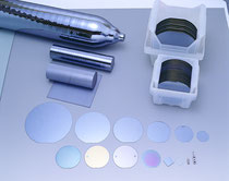
- Corresponding 2inch to 12inch (Even small amounts can be accommodated)
- Special size, FZ wafers are also available.
- Provide high quality wafers under through quality control.
- Materials and processing are provided at “low price and short delivery time”.

Silicon (Si) wafer application
→ For dummy, for monitoring, for solar
*Thermal oxide film processing is also available.
*Wafer with various film (by PVD, CVD equipment) is available as well.
Distinction between dummy and monitor
Specifications other than size, thickness are not mentioned, please specify dust not mentioned or dust free. (Wafer characteristics can be specified at delivery.)
- Monitor wafer
Please specify on quotation request form.
*In order to promptly secure materials, we ask for cooperation in expanding the range of resistivity and thickness.
About regeneration processing
By carrying out regeneration processing (lap, etching, chemical polishing) on the wafers used, such as wafers used for transport tests and defective wafers generated during the process, the particle level and surface condition are restored to before use state. Please contact us as we can suggest the best regeneration method depending on the condition you are using.
Other handling substrates
- Ge and Si, ZnSe *Infrared material (supply of lens and flat plate)
- Epi, SOI, SiC
- Quartz, Pyrex, Tempax, Sapphire
- Various compound semiconductor substrates (Si-GaAs, GaP, InP, LiTaO3, LiNb3)
- Ceramics (sapphire, crystal, ferrite, high purity alumina, zirconia)


Silicon wafer inventory sales
*note
1.Specifications:Specification details will be confirmed at the time of quotation after inquiries.
2.Delivery time: About one week after order receipt (re-inspection, reprocessing, wafers not on the list are consulted separately)
3.When making an inquiry, please tell us lot number or inquiry number.
4.Since it will be in order of first come first served, stock may be gone after inquiries.


