


パターニング加工
当社では、半導体素子、MEMS構造、めっき、エッチング(Deep-RIE、Dry&Wet)用のレジストパターニングの手法としてアライナー、ステッパー、EBでの露光・現像が可能です。
ポジ型、ネガ型、ドライフィルム、薄膜、厚膜用各種レジストを所有しております。ポリイミドのパターニングも可能です。

アライナー
- 3インチ~12インチ対応可能
- 等倍コンタクト露光
- リフトオフ用逆テーパーパターン
- 裏面アライメント
- レジスト以外にも低応力絶縁樹脂もパターニングも可能


ステッパー
- i線、KrF、液浸対応可能
- 4~12インチ対応可能(3インチ以下は別途ご相談)
- i線ステッパーは1shot44㎜角の高スループット
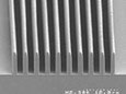
高アスペクトレジスト、厚膜レジスト形成
- 高アスペクト比対応レジスト(配線形成用)
- 厚膜レジスト(Cuピラー用)
- その他Ni電鋳用高アスペクト比レジストも取り扱い中
レーザー直描
- 基板サイズ610㎜×510㎜まで対応可能
- アライメント(赤色、緑色、赤外の3種)可能
- 高スループット
- 直描の為マスク不要
- L&S8μm
EB(直接描画)
- 80nm以下のパターニングが可能


